https://scottyspectrumanalyzer.us
https://groups.io/g/spectrumanalyzer
http://www.qsl.net/bg6khc/my_version2.htm
You find here all about Calibrating the MSA and my Modifications.
The need of a Spectrum Analyzer
Due to my GHz experiments (see ADF4351 project) I found that I need a Spectrum Analyzer… You can buy one (very expensive) or build one (a lot of work). I choose for the last option.
I searched the internet (again!) and found an interesting project to build a (wide range) spectrum analyzer (the Scotty spectrum analyzer). The original project was started in 2001 and is still very popular. The decision was very fast made…. I will start this project.Because I already was in contact with Yanjun BG6KHC, I knew that he has a complete set of PCB’s for the SLIM-MSA available. Even better: he sells a kit for this SA (PCB’s, enclosures and 64 MHz TCXO). Together with a hobby friend of my, we both ordered a kit and I start collecting for both of us the required parts from Digikey, Mini Circuits and e-bay.
After 2 month of collecting parts and getting the SA kits from China to Holland, we finally get starting building the SA.
USB to LPT Converter
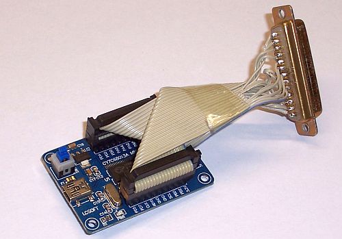
Because I wanted to control the MSA by USB, I needed an USB to LPT converter. I read on the forum that they used a Cypress CY7C68013A-56 EZ-USB FX2LP USB 2.0 Develope Board board for it, which was very cheap, available on e-bay. So I bought one, programmed it and it seems to work. I have tested the interface with the LPT test utility in the MSA software and the interface is working well. I can program all the (LPT) databits by means of the test program.
Note: Please read the warning on the forum about this board because some boards have a counterfeit Cypress chip installed!!The Cypress CY7C68013A-56 board with connected D25 plug
Start building and testing the MSA modules
I will briefly described the building and testing of each module and I add notes and special attentions where there are differences between the original schematics of Scotty and the PCB’s made by Yanjun. I hope this helps you in successful building the MSA with the PCB’s of Yanjun.
I did the test in the same order as Scotty described on his test page: http://www.scottyspectrumanalyzer.com/testingslim.htmlThe modules should be inserted in an enclosure and therefore I had to make one side panel fit for the SMA connectors and one new panel made from PCB board to solder the feed-thru condensers in it. Of course this is not necessary when you are using feed-thru capacitors with a mounting nut, as Yanjun did.
Enclosure and pcb board panel
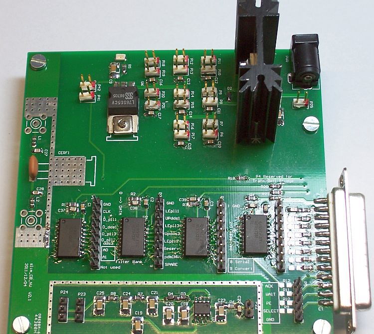
Control Board (SLIM-CB_NV)
Starting with the Control Board we discovered that Yanjun had replaced the DIL 74ACT573 IC’s by SOP parts… Oops, we had the wrong type and should buy new ones. If you buy SOIC parts by accident, no worry, if you bent the legs a bit to the inside, the chip just fits over the small pads on the PCB.Because of the use of the Cypress USB-LPT converter we had to make some small modifications but these are very well described on the SLIM-MSA site and they have no negative effect if you are using LPT1.
Testing: Before you start testing the control board, download the files as described on http://www.scottyspectrumanalyzer.com/msasetcal.html and don’t forget to download and install the modified LPT1 drivers (Redist.zip). Installation is described in the file ReadMe116.txt.
I have tested the board with the LPT1 connection and the USB interface as well. In both set-ups the data bits on connector P1 – P3 are programmable.
Be aware that when there is no LPT cable or USB interface connected to the board, it’s possible that there is some wild oscillating of the 74ACT573’s and the total current could increase to more than 100 mA!!MSA Control board
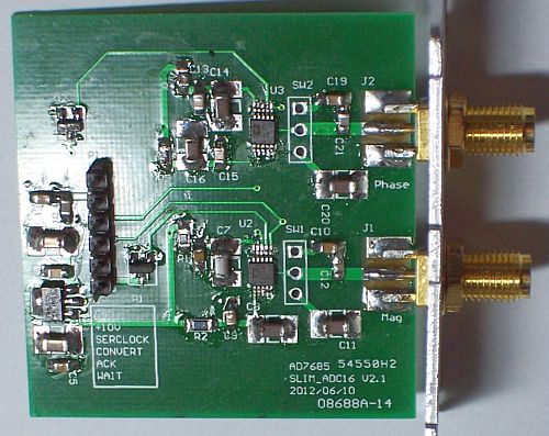
16 bit A to D Converter (SLIM-ADC16)
Notes: If the SLIM-ADC-16 has been constructed for use in the Basic MSA only, the U1 voltage regulator will be installed. If constructed for the MSA/VNA, U1 may be omitted. If so, the SLIM-PDM module’s 5 volt power can supply the ADC module. Make sure the PDM module has its ferrite jumpers installed (FBx and FB2).
The Magnitude and Phase filtering is done by softwareSelecting the capacitors that filter Magnitude and Phase.
– Wide: both switches are open
– Mid: Mag and Phase are connected to the 0,1 μF capacitor
– Narrow: Mag and Phase are connected to the 10 μF capacitor16 bit A/D Converter
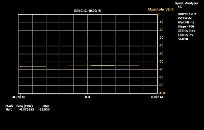
Testing: Before testing I added temporary mini switches on the board. I have tested the board according the test description on Scotty’s site and all the tests are OK!
Phase test
Magnitude test
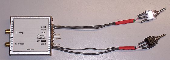
Later on I added two switches to the front panel for setting the Video- and Phase Filter. I used shielded cables to the switches and according to Scotty’s remarks: if you don’t make the wires to long it’s no problem….
ADC-16 with Video Filter switches
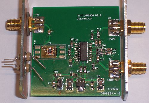
Logarithmic Detector (SLIM-LD-8306)
Yanjun had made a modification to his original V2 board (V2.2) to make it possible to use a smaller impedance transformer (TC16-161TG2 from Mini circuits).Notes: As you can see I have added a 0,1μF capacitor between J1 and T2 as suggested by Scotty in his test page. Be aware that the footprint of T2 on the PCB is up-side-down. The center tap of T2 is on the wrong site. The orientation white dot on T2 should be on the same site as J1.
Note to RF leakage: This module is also very sensitive for RF radiation. I used a ferrite bead on the 10V wire and installed an extra decoupling C of 0.1uF near the 10V feed-thru condensers. I also filled the gap between the board and the PCB made cover with very thin copper plate.
Logarithmic Detector
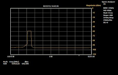
Testing: All performed tests are according the manual. Values of Magdata bits are for step 8: 4785 and for step 10: 4768.
Test step 9 results (finger on J1)
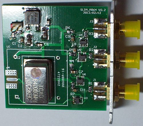
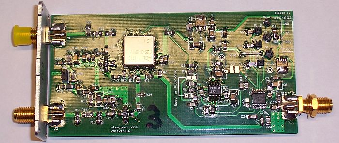
64 MHz Master Oscillator (SLIM-MO64)
The next module to be build was the 64 MHz master oscillator. The output signal on the 3 SMA connectors is about +17 dBm @ 64 MHz.
MSA 64 MHz Master Oscillator with TCXO
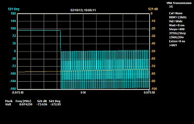
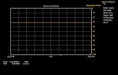
Testing: The given values in the test manual correspond to the measured values. Below the MO64 output signal with an attenuation of 30 dB. Also 10 dB steps up or down with the attenuator corresponds exactly with the reading on the screen.
MO64 signal output with 30dB attenuation
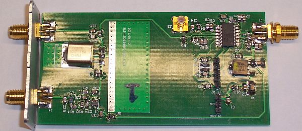
DDS-1 and DDS-3 (SLIM-DDS9850)
These two modules are rather easy to build, except placing the AD9851.. You must have stable fingers and very good eyes. I used a magnifying glass mounted on my glasses and solder the AD9851 nearly with my nose on the solder iron….
Notes: The PCB’s are already prepared for serial control of the AD9851. So only data BD7 is needed. J3 is not used but I have put a SMA connector on it for measurement purposes.DDS-1 and DDS-3
Testing: The DDS won’t work at the first test. I had skipped the 100 pF C’s at C22, C24 and C25 (C23, C24 and C25 on the schematic) because of the (later) use of feed trough capacitors in the enclosure. But that was not a good idea… The 100 pF capacitors are needed to bring the data and clock lines to a higher level. After I placed the capacitors the DDS1 an 3 was working perfect!
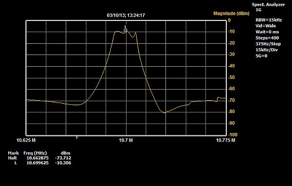
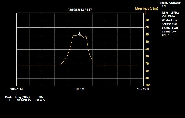
DDS1+ Final Crystal Filter sweep test on 10.7 MHz
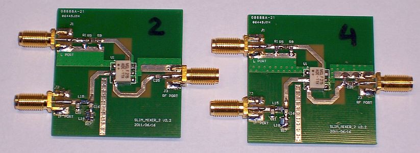
Mixers (SLIM-MXR-1 / MXR-4)
The four mixer PCB’s are easy to assemble. Use for mixer 1 and 3 SLIM_MIXER_1 PCB and for mixer 2 and 4 SLIM_MIXER_2 PCB.
Notes to MXR_3: R25 = C25 on the PCB. For R21 and R29 are only the pads on the board, not the identification. Solder C29 against R29.
Notes to MXR_4: R25 = C25 on the PCB. Solder R21 and R29 just left and right from R25. There are no pads on the PCB for these resistors.MSA mixers 1 and 3
MSA mixers 2 and 4
Testing: I have tested the mixers according Scotty’s test page and found an Insertion Loss of about 9.1 dB. I wonder if it has something to do with the extra 2.5 dBm attenuation in the mixers…
Mixer 4 output during mixer test
Mixer I/R Isolation (dBm) Output at J3 (dBm) Insertion loss (dBm) 1 -54.8 -16.6 9.1 2 -56.1 -17.4 9.9 3 -68.9 -30.6 9.1 4 -65.0 -31.4 9.9 PLO-1 and 3 (SLIM-PLO1 and 3)
This modules are hard to built. There are a lot of parts on it and the PCB is gold plated on which the solder is not easily flow. Using solder flux may help.
Notes: Solder the pads of the ROS-2150VW before placing this part. R50, R70 and D70 are not needed and therefore not installed!
On the PCB C21 through C23 are missing because when you are using feed trough capacitors they are not necessary. But for testing purposes it’s better to install them on the PCB. You can use 1206 SMD types.PLO-1 (and 3)
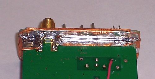
Preventing RF Leakage
During testing the MSA in my final enclosure, I found a serious problem: RF Leakage! I discussed that with Scotty and he advised me to pay special attention to the feet-thrus capacitors and the mounting of the cover (made by double sided pcb) to the PLO PCB.
Because of the 100pF capacitors on the PLO-PCB, I used 0 pF feed-thru in the cover to prevent overload of the data wires. That was not such a good idea… I removed the caps from the PLO PCB and replaces the feed-thru by 100pF pieces.
I also add ferrite beads with 2 turns of thin copper wire between the feed-thru and the connection on the PLO PCB. That differs about 40dB (!) in radiation of the data wires! Also put a ferrite bead on the 10V and 20V wires between the feed-thru and the connection on the PLO board.
You can test this very easy by making a ‘sniffer’ with a 1cm loop mounted on a MSA connector and connect that to the input of mixer 2. Run your MSA, sweep set to 0 MHz at Center and Span and search for transmitting wires.Upper side PLO board with ferrite beads
lower side PLO board with thin copper gap fill
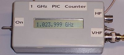
Testing: Below you see the test set-up to test PLO1 and PLO3. The frequency output is in my case 1013.258 MHz (depending of settings in MSA).
Total power consumption in this test set-up is about 250 mA @ 12 Volt.PLO-1 test set-up.
PLO-2 (SLIM-PLO2)
PLO-2 has less parts so it’s easier to built as PLO-1, but watch out, especially where the PCB is marked with note ‘Used for PLO2 only’. I have made a close-up to see how these parts should be placed.
Notes: R3 = R4 on the schematic and C15 is placed below the not used pads of R2. B.T.W. R3 can also placed on the pads between the small white square on the PCB, see the detail picture below.
C21 through C23 are missing on the PCB, there are some pads near the LE and Data lines which can be used but the one at the Clock line is too far away.Detail of difference between PLO2 and PLO 1 and 3
Testing: The PLO-2 is working fine. After start-up of the MSA software, the output was 1023.999 MHz.
PLO-2 frequency
PLO Frequency and RF Power test
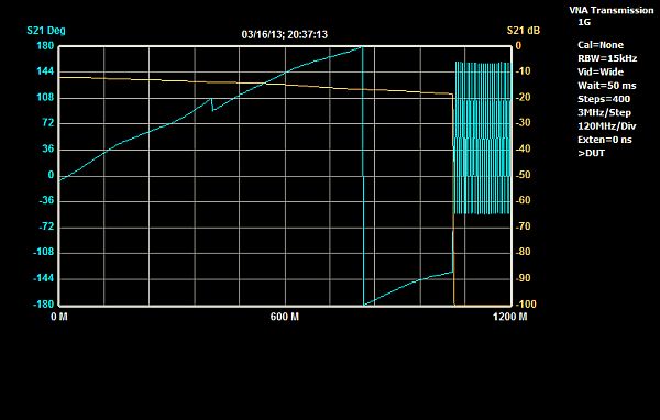
This test is a kind of integration test but without the cavity filter. The test is testing PLO-1, PLO-2 and PLO-3 together with DDS-1 and DDS-3 and Mixer-2. The result should be the Final Xtal Filter characteristics. The PLO frequencies are:
PLO-1: 1013 MHz (sweep)
PLO-2: 1024 MHz
PLO-3: 1024 MHzFinal X-tal Filter characteristics during PLO integration test
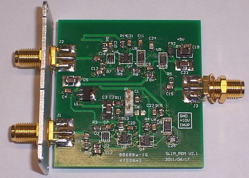
Phase Detector (SLIM-PDM)
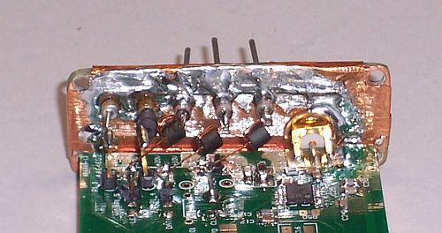
This module is hard to build because of the very small IC’s. If you accidentally have shortened the legs of U5, U8 or U9, you can easily correct that with small desoldering braid.Note to RF leakage: This module is also very sensitive for RF radiation. I have used a ferrite bead with 2 turns of wire between the 100pF feed-thru and the INVP connection on the PDM board. I also used a ferrite bead on the 10V wire and installed an extra decoupling C of 0.1uF near the 10V feed-thru condensers. I also filled the gap between the PDM board and the PCB made cover with very thin copper plate. This decreases the RF radiation with about 20 dB (thanks to Scotty!).
Phase detector
Testing: This is the last module to test. Before I had to, I have modified the ADC-16 unit by removing the 5 Volt regulator. The ADC-16 became his power from the PDM module, necessary for using the MSA in VNA mode. Below you see the test results.
Test result of PDM module testing
Setup during PDM module testing
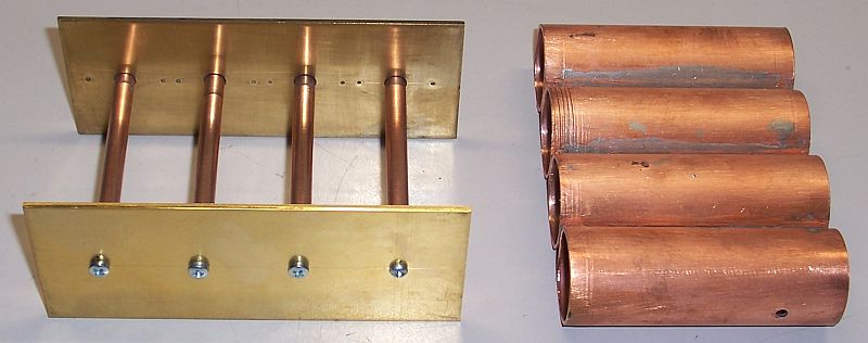
Cavity filter
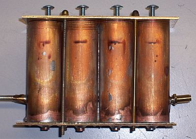
Now I started with the cavity filter on 1013 MHz. It was not easy to solder the 4 tubes to each other in a way that they are straight and upright. I used my vertical drilling machine to drill the holes in the horizontal mounting plates and also through the 4 soldered tubes. These holes are for the semi-rigged coax hair-pin loops.Mounting plates, resonators and cavity tubes
An attempt to silver-plate the resonators and the inside of the tubes ended in a disappointment… I used HG Silver polish, but after various attempts there was not a shade of silver on it…..
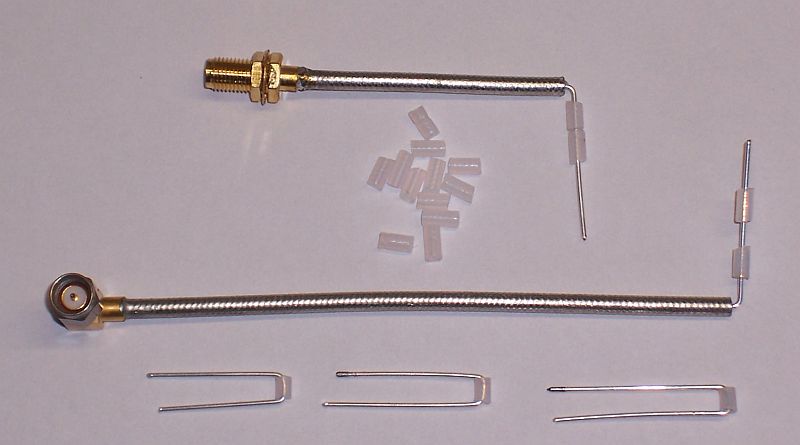
Next step was making the SMA semi-rigid cables, hairpin couplers and spacers. I made it all from SMA semi-rigid cable bought on e-bay.
SMA semi-rigid cables, hairpin couplers and spacers
Then I had to bring the hairpin couplers and SMA semi-rigid cables in place and solder the copper tubes to the bottom plate . To prevent separating the 4 tubes during soldering I had made some clamps to hold the tubes together if the solder between the tubes possibly melts. That part of the job finished successful! But unfortunately I broke one of the semi-rigid cables and I had to replace that with a connector soldered directly on the copper tube. I found that the kind of semi-rigid I used is not easy to solder. It’s better to use solid copper shielded semi-rigid in stead of semi-rigid with a braided shield.
The four tubes soldered to the bottom plate
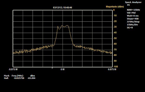
I clamped the upper plate in place with 4 long M3 screws and start to test if the filter was tunable to 1013 MHz. And indeed, it was! The next step was to test the filter in the MSA. I setup the modules as described in part S-B of Scotty’s test page.
After some tuning with the four tuning screws I have got a nice shape but the insertion loss is too high (about 8.5 dB). Maybe this is caused by the not yet soldered upper plate.Cavity filter test in MSA set-up
Note to preventing RF leakage: I found that the not-soldered upper plate, in spite of the very good closing of the plate to the 4 tubes, was a very good receiver of unwanted RF! I did not get the nice shape as in the above picture. After I had soldered the plate to the tubes (fortunately nothing went wrong..) the shape was again perfect and the insertion loss was improved with 1.5 dB!
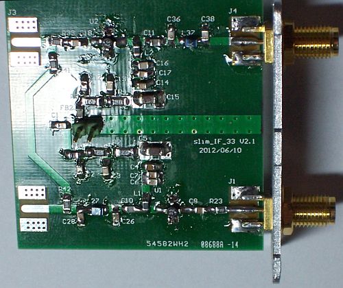
You can test the RF leakage around the filter by yourself by using the ‘sniffer’ as a transmitter. Connect the sniffer to the TG output and set the RF generator in the Sweep Parameters Window to 1013.3 MHz. Run the MSA and search where the magnitude increases due to RF leakage.I.F. Amplifier (SLIM-IF-33)
This is a 2 times 20 dBm amplifier @ 10.7 MHz. Because of the use of both amplifiers in cascade, Yanjun has made an internal connection between J2 and J3 by means of two 0 ohm resistors (R41 and R42). Connectors J2 and J3 are not used.
Attention: J1 = Input (J3 at MSA) and J4 = Output (J2 at MSA)I.F. Amplifier
Testing: The overall gain is 38,7 dBm @ 10.7 MHz.
Upper part is the RF generator (at -40dBm), below is the RF measuring receiver (PSM-5)
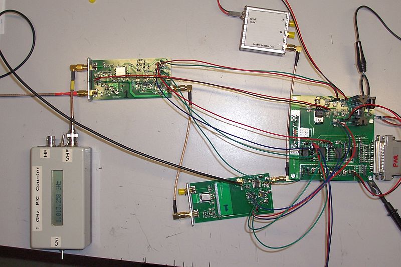
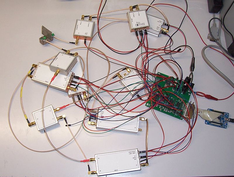
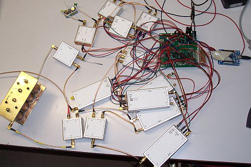
Connecting all the modules together, being a spectrum Analyzer…
Now all the modules are ready and tested, I had to connect all the modules together and to the Control Board to see if it’s a Spectrum Analyzer!A spectrum Analyzer…
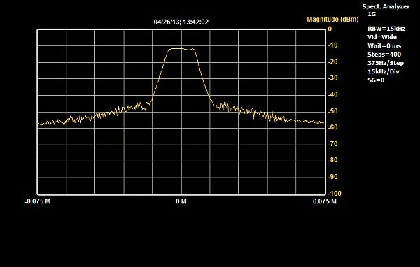
After starting the MSA software, the first thing I saw was the Final X-tal filter response. Because I did not like the shape, I replaced the filter by an other one and matched it to 50 ohm. Below you see the results, much better then before.
Retuned final x-tal filter
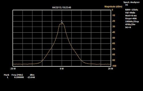
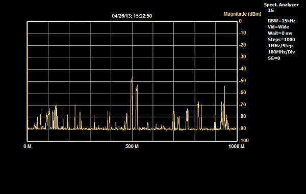
Then I set the sweep from 0 to 1 GHz and connect my vertical antenna to the input of the SA. Yes, the SA was working! I saw the complete spectrum with the local FM stations, GSM etc etc.
1 GHz spectrum on a Diamond vertical
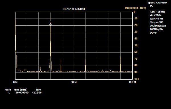
Connecting my RF generator gives also a nice picture and about 10 dB above the level of the generator (the MSA is not calibrated yet).
RF generator on 30 MHz @ -30 dBm
Resolution filters
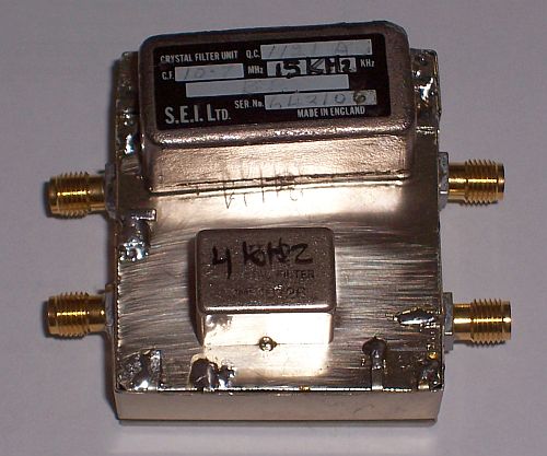
I build some resolution filters in an enclosure. A 15 KHz and 7.5 KHz X-tal filter fit in a small brass enclosure where I soldered SMA connectors on. I matched the filters with serial L and parallel trim C.Resolution filters 15KHz and 7.5 KHz (top view)
Resolution filters 15KHz and 7.5 KHz (insight view)
I’m planned to build a 100KHz and 1 MHz resolution filter as well. Switching the filters with the filter switch of Sam Wetterlin.
Note: Pay serious attention to make all the compartments leakage free. There should be no leakage between the 2 compartments and also not between the in- and output connectors.
Building the MSA in an enclosure
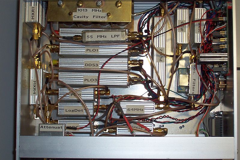
From a friend of mine I have got an enclosure (29 x 23 x 10 cm) which meets my requirements. I start making a sketch where the modules should be placed. In all modules I drilled (using a template) two holes, make M3 thread in it and mount the module on the bottom plate. There was just enough room for all the modules. As you can see, I have mounted the control board and USB interface vertical against the right-hand panel.Enclosure with all the modules (X-tal module removed for testing)
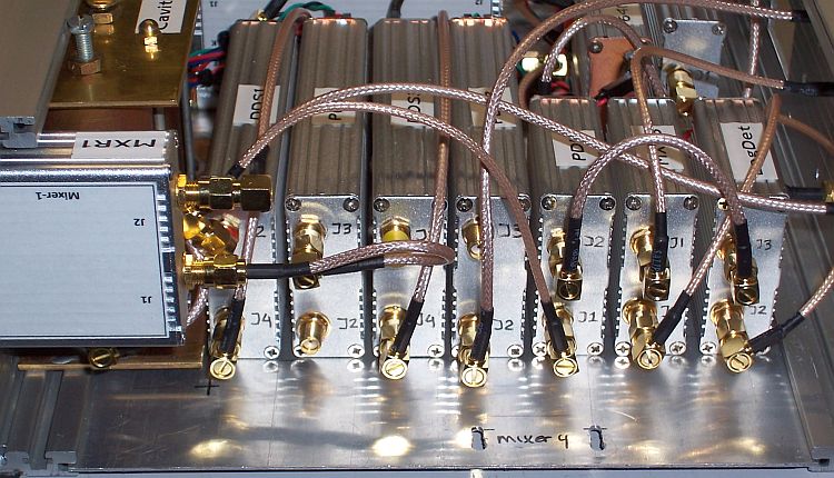
Module interconnections (Mixer 4 removed)
Testing the MSA in it’s new ‘home’.
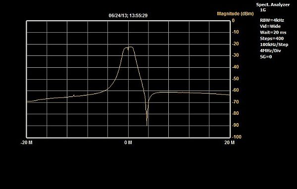
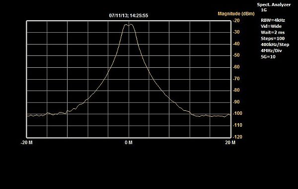
During test I found that the the cavity filter shape was ‘not as nice’ as it was during earlier tests. I had an 1,5 hour very interesting Skype talk with Scotty about that issue. Conclusion: Inside- and outside cross-talk was bothering me! Scotty advised me to take special attention to RF leakage of the modules, especially at the PLO modules. After his story I can understand that the PCB made covers are a bit leaking RF energy (as Scotty said: fill up the module with water and take a look where the water comes out… there you have RF leakage!)
Read at the concerning modules what I have done to get rid of this RF leakage.Malformed cavity filter shape due to Cross-talk
Cavity filter shape after leakage repair